Vazquez, M.; Connolly, JP.; Cubero García, OJ.; Daly, G.; Halm, A.; Kopecek, R.; Mihailetchi, V.... (2011). Cost model for LIMA device. Energy Procedia. 8:443-448. https://doi.org/10.1016/j.egypro.2011.06.163
Por favor, use este identificador para citar o enlazar este ítem: http://hdl.handle.net/10251/69176
|
Título:
|
Cost model for LIMA device
|
|
Autor:
|
Vazquez, M.A.
Connolly, James Patrick
Cubero García, Oscar Jesús
Daly, G.
Halm, A.
Kopecek, R.
Mihailetchi, V.D.
Pérez Mayor, Ester
Pucker, G.
Sánchez Plaza, Guillermo
Pavesi, L.
|
|
Entidad UPV:
|
Universitat Politècnica de València. Instituto Universitario de Tecnología Nanofotónica - Institut Universitari de Tecnologia Nanofotònica
|
|
Fecha difusión:
|
|
|
Resumen:
|
[EN] In this paper we show the results of the cost model developed in LIMA project (FP7-248909). The LIMA project is titled "Improve photovoltaic efficiency by applying novel effects at the limits of light to matter ...[+]
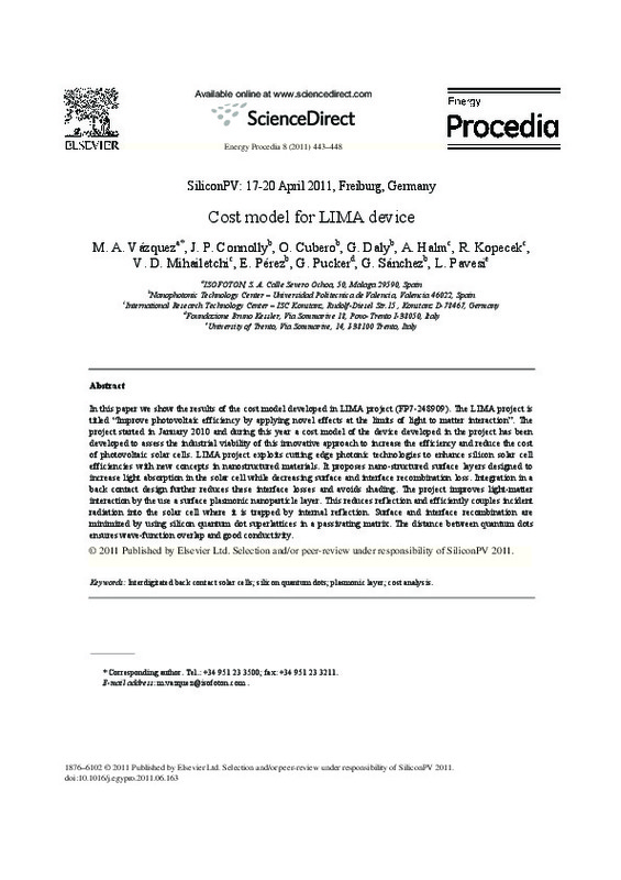
[EN] In this paper we show the results of the cost model developed in LIMA project (FP7-248909). The LIMA project is titled "Improve photovoltaic efficiency by applying novel effects at the limits of light to matter interaction". The project started in January 2010 and during this year a cost model of the device developed in the project has been developed to assess the industrial viability of this innovative approach to increase the efficiency and reduce the cost of photovoltaic solar cells. LIMA project exploits cutting edge photonic technologies to enhance silicon solar cell efficiencies with new concepts in nanostructured materials. It proposes nano-structured surface layers designed to increase light absorption in the solar cell while decreasing surface and interface recombination loss. Integration in a back contact design further reduces these interface losses and avoids shading. The project improves light-matter interaction by the use a surface plasmonic nanoparticle layer. This reduces reflection and efficiently couples incident radiation into the solar cell where it is trapped by internal reflection. Surface and interface recombination are minimized by using silicon quantum dot superlattices in a passivating matrix. The distance between quantum dots ensures wave-function overlap and good conductivity. © 2010 Published by Elsevier Ltd.
[-]
|
|
Palabras clave:
|
Cost analysis
,
Interdigitated back contact solar cells
,
Plasmonic layer
,
Silicon quantum dots
,
Back contact
,
Cost models
,
Cutting edges
,
Incident radiation
,
Innovative approaches
,
Interdigitated back contacts
,
Internal reflections
,
Light-matter interactions
,
Matrix
,
Nanostructured surface
,
Photo-voltaic efficiency
,
Photonic technologies
,
Photovoltaic solar cells
,
Plasmonic
,
Plasmonic nanoparticle
,
Quantum dot superlattices
,
Solar cell efficiencies
,
Surface and interfaces
,
Cost accounting
,
Costs
,
Crystalline materials
,
Efficiency
,
Incident solar radiation
,
Nanostructured materials
,
Photovoltaic effects
,
Plasmons
,
Semiconductor quantum dots
,
Solar power generation
,
Surfaces
,
Cost benefit analysis
|
|
Derechos de uso:
|
Reserva de todos los derechos
|
|
Fuente:
|
Energy Procedia. (issn:
1876-6102
)
|
|
DOI:
|
10.1016/j.egypro.2011.06.163
|
|
Editorial:
|
Elsevier
|
|
Versión del editor:
|
http://dx.doi.org/10.1016/j.egypro.2011.06.163
|
|
Título del congreso:
|
1st International Conference on Crystalline Silicon Photovoltaics (SiliconPV)
|
|
Lugar del congreso:
|
Freiburg, Germany
|
|
Fecha congreso:
|
APR 17-20, 2011
|
|
Código del Proyecto:
|
info:eu-repo/grantAgreement/EC/FP7/248909/EU/Improve Photovoltaic efficiency by applying novel effects at the limits of light to matter interaction/
|
|
Agradecimientos:
|
This work has been carried out in the framework of the LIMA Project. The EC is gratefully acknowledged for financial support under Contract number FP7-248909.
|
|
Tipo:
|
Artículo
Comunicación en congreso
|


